CSCI 110, Spring 2011
Home | | Course Schedule | | Assignments | | Lecture NotesLab 7 solution
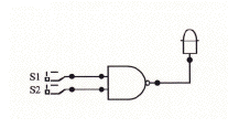
Experiment 1: Step 1: Wire the circuit shown in the schematic diagram above using a "Logic Switch" and a "Logic Display". Be careful to wire it as shown in the diagram. If you need help using CircuitMaker at any point along the way refer to the appropriate on-line help.
Step 2: Click on the "Run" button in the Toolbar. Now move the mouse until it is
pointing at the switch. Click on the switch several times and observe that it moves
up and down. This is a special type of switch which outputs a logic 0 when down
and a logic one when up. Use the mouse to change the switch to a logic 0.
What
do you observe on the Logic Display?
-
Answer: The light on the LED is off.
Step 3: Use the mouse to change the switch to a logic 1.
Now what do you
observe on the Logic Display?
-
Answer: The light on the LED is on.
Step 4: Select thc "Delete Tool" from the Toolbar. Now point at the wire between
the switch and the Logic Display and click. Now click on the "Run" icon in the
Toolbar.
What do you observe on the Logic Display now?
-
Answer: The light on the LED is off.
Step 5: Change the switch to a logic 0.
Now what do you observe on the Logic
Display?
How can you easily tell what logic state is present at any point in a
circuit at any time?
-
Answer: The light on the LED is off.
You can tell what logic state is present by attaching an LED and looking to see whether the light is on or off. If it is on, the logic state is 1. If it is off, the logic state is 0.
Experiment 2:
In this experiment you will use the AND gate. You will learn what the truth table
for the AND gate is by experimental methods.
Wire the circuit as shown below using the following devices:
-
2-Input AND, Logic Display, Logic Switch
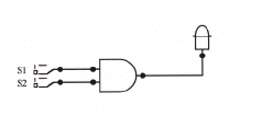
| S1 | S2 | Output of AND |
| 0 | 0 | 0 |
| 0 | 1 | 0 |
| 1 | 0 | 0 |
| 1 | 1 | 1 |
You have now discovered the truth table for the AND gate. Can you see why it is called an AND gate? It's because both input one AND input two must be at a logic 1 in order for the output to be a logic 1. Can you guess what the truth table for the OR gate might be? Proceed to the next experiment to see if you are right.
Experiment 3:
The purpose of this experiment is to learn what the truth tables for the OR,
INVERTER, NAND, NOR, and XOR gates are. These gates are fundamental to
almost all digital circuits and understanding their truth tables is a prerequisite to
gaining an in depth understanding of digital electronics. Spend as much time as is
required to thoroughly understand these devices. It will pay off later by allowing
you to use your creativity to design circuits on your own.
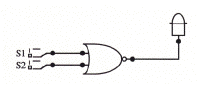
Wire the circuit shown below for the OR gate.
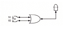
Fill in the truth table below for the OR gate by changing the switches to all four possible combinations and recording the output state in the following truth table.
| S1 | S2 | Output of OR |
| 0 | 0 | 0 |
| 0 | 1 | 1 |
| 1 | 0 | 1 |
| 1 | 1 | 1 |
Wire the circuit for the INVERTER and then fill in its truth table.
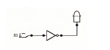
| S1 | Output of Inverter |
| 0 | 1 |
| 1 | 0 |
Wire the circuit for the NAND gate and then fill in its truth table.
| S1 | S2 | Output of NAND |
| 0 | 0 | 1 |
| 0 | 1 | 1 |
| 1 | 0 | 1 |
| 1 | 1 | 0 |
Wire the circuit for the NOR gate and then fill in its truth table.
| S1 | S2 | Output of NOR |
| 0 | 0 | 1 |
| 0 | 1 | 0 |
| 1 | 0 | 0 |
| 1 | 1 | 0 |
Wire the circuit for the XOR gate and then fill in its truth table.
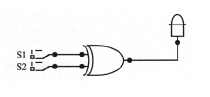
| S1 | S2 | Output of XOR |
| 0 | 0 | 0 |
| 0 | 1 | 1 |
| 1 | 0 | 1 |
| 1 | 1 | 0 |
Experiment 4:
The purpose of this experiment is to gain some experience wiring together
more than one logic component. The circuit below is wired to compute the
following:
(S1 AND NOT S2) OR (S2 AND NOT S1)
Wire the circuit shown below and fill in the truth table.
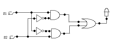
| S1 | S2 | Output of Circuit |
| 0 | 0 | 0 |
| 0 | 1 | 1 |
| 1 | 0 | 1 |
| 1 | 1 | 0 |
The above truth table should match the truth table for one of the above logic gates. Which single gate's truth table does it match?
-
Answer: It matches the XOR gate.