MONT 113G, Spring 2012
Home | | Course Schedule | | Assignments | | Lecture NotesLaboratory 1
Due at the end of today's class
Experiment 1: The purpose of this experiment is to demonstrate what a logic 0 and logic 1 state are within a circuit by using the Logic Switch and Logic Display devices. You will also learn the necessity of wiring components together correctly in a circuit in order for the circuit to function as planned.
Digital circuits operate based on two possible logic levels present in the circuit. These logic levels are logic 0 and logic 1. Logic levels 0 and 1 (also known as low and high levels) refer to voltage levels and for the type of integrated circuits available. In CircuitMaker these levels are typically 0 volts and about 5 volts respectively. Because digital circuits operate based on only two levels, learning the basics of digital circuit theory and design is not difficult. The logic 0 and logic 1 are the control signals which will cause all integrated circuits to operate. The operation of a digital circuit can be visualized by imagining a black box into which various control signals are passed (logic levels 0 and 1) and out of which some other combination of logic levels comes.
The Logic Display is a simple device used in CircuitMaker to indicate the state of any given node or point in a digital circuit. Typically, however, in a real digital logic circuit you would use a Light Emitting Diode (LED) which, when its node is connected through a current limiting resistor to +5V and its cathode is pulled to a low state, will emit light. LED's are widely used as display indicators in everything from personal computers to stereos. They are used to show such things as power is applied and that a cycle has finished. LED's are available in several colors such as red, green, and yellow.
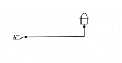
Step 1: Wire the circuit shown in the schematic diagram above using a "Logic Switch" and a "Logic Display". Be careful to wire it as shown in the diagram. If you need help using CircuitMaker at any point along the way refer to the appropriate on-line help.
Step 2: Click on the "Run" button in the Toolbar. Now move the mouse until it is
pointing at the switch. Click on the switch several times and observe that it moves
up and down. This is a special type of switch which outputs a logic 0 when down
and a logic one when up. Use the mouse to change the switch to a logic 0.
What
do you observe on the Logic Display?
Step 3: Use the mouse to change the switch to a logic 1.
Now what do you
observe on the Logic Display?
Step 4: Select thc "Delete Tool" from the Toolbar. Now point at the wire between
the switch and the Logic Display and click. Now click on the "Run" icon in the
Toolbar.
What do you observe on the Logic Display now?
Step 5: Change the switch to a logic 0.
Now what do you observe on the Logic
Display?
How can you easily tell what logic state is present at any point in a
circuit at any time?
Experiment 2:
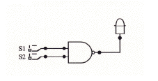
The purpose of this experiment is to learn what an AND gate is and what the truth
table for it is.
Integrated circuit gates are the fundamental building blocks or digital circuits. A gate is simply an integrated circuit which produces specific outputs for any given input condition. There are six types of gates that are very common in digital circuits. They are the INVERTER, the AND gate, the OR gate, the NAND gate, the NOR gate, and the XOR gate. These gates are available as integrated circuits which combine several gates into one package. The AND gate for example can be purchased at any local electronics store as an integrated circuit called the 74LS08 and this one IC contains four AND gates in the same package. The name 74LS08 is derived by the manufacturer and is numerical in order to make it easy to keep track of a wide variety of IC's.
The term gate is used because these devices serve as an entrance through which signals in a circuit pass. A gate can be pictured as a device into which digital signals enter and which has an output or outputs from which new signals come. The resulting signals out of a gate depend on what the input signals were and are based on a very precise set of rules called a truth table. Each type of gate has its own truth table which determines what the outputs will be given any set of inputs.
In this experiment you will use the AND gate. You will learn what the truth table for the AND gate is by experimental methods.
Wire the circuit as shown below using the following devices:
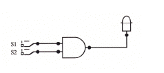
| S1 | S2 | Output of AND |
| 0 | 0 | |
| 0 | 1 | |
| 1 | 0 | |
| 1 | 1 |
You have now discovered the truth table for the AND gate. Can you see why it is called an AND gate? It's because both input one AND input two must be at a logic 1 in order for the output to be a logic 1. Can you guess what the truth table for the OR gate might be? Proceed to the next experiment to see if you are right.
Experiment 3:
The purpose of this experiment is to learn what the truth tables for the OR,
INVERTER, NAND, NOR, and XOR gates are. These gates are fundamental to
almost all digital circuits and understanding their truth tables is a prerequisite to
gaining an in depth understanding of digital electronics. Spend as much time as is
required to thoroughly understand these devices. It will pay off later by allowing
you to use your creativity to design circuits on your own.
Wire the circuit shown below for the OR gate.
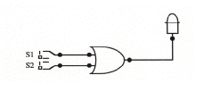
Fill in the truth table below for the OR gate by changing the switches to all four possible combinations and recording the output state in the following truth table.
| S1 | S2 | Output of OR |
| 0 | 0 | |
| 0 | 1 | |
| 1 | 0 | |
| 1 | 1 |
Wire the circuit for the INVERTER and then fill in its truth table.
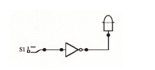
| S1 | Output of Inverter |
| 0 | |
| 1 |
Wire the circuit for the NAND gate and then fill in its truth table.
| S1 | S2 | Output of NAND |
| 0 | 0 | |
| 0 | 1 | |
| 1 | 0 | |
| 1 | 1 |
Wire the circuit for the NOR gate and then fill in its truth table.
| S1 | S2 | Output of NOR |
| 0 | 0 | |
| 0 | 1 | |
| 1 | 0 | |
| 1 | 1 |
Wire the circuit for the XOR gate and then fill in its truth table.
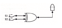
| S1 | S2 | Output of XOR |
| 0 | 0 | |
| 0 | 1 | |
| 1 | 0 | |
| 1 | 1 |
Experiment 4:
The purpose of this experiment is to gain some experience wiring together
more than one logic component. The circuit below is wired to compute the
following:
(S1 AND NOT S2) OR (S2 AND NOT S1)
Wire the circuit shown below and fill in the truth table.
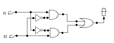
| S1 | S2 | Output of Circuit |
| 0 | 0 | |
| 0 | 1 | |
| 1 | 0 | |
| 1 | 1 |
The above truth table should match the truth table for one of the above logic gates. Which single gate's truth table does it match?
What To Turn In.